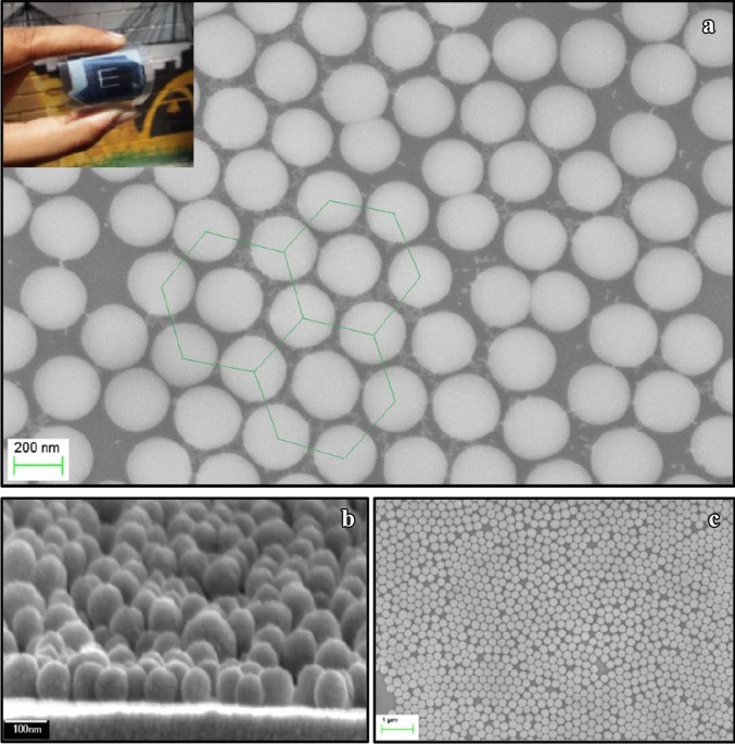
a) SEM image of crystallized silica spheres on a plain Si substrate.

Download scientific diagram | (a) SEM image of crystallized silica spheres on a plain Si substrate. The small black and large white squares represent the areas used for the calculation of the Fourier transforms in Figure 3c and d. (b) Optical micrograph of the etched substrate after the crystallization of silica opals (about 1 mm × 0.7 mm). The high-lying parts of the wafer are uncovered (blank silicon ) white); the low-lying etched pattern is completely filled (dark). (c, d) Representative SEM images showing the same selectivity. Notice the difference between isolated trenches and trenches of the same size, which are connected to a continuous trench in part d. from publication: Integration of Self-Assembled Three-Dimensional Photonic Crystals onto Structured Silicon Wafers | We report on the fabrication of high-quality opaline photonic crystals from large silica spheres (diameter of 890 nm), self-assembled in hydrophilic trenches of silicon wafers by using a novel technique coined a combination of "lifting and stirring". The achievements reported | Silicon Wafer, Photonic Crystals and Self-Assembly | ResearchGate, the professional network for scientists.

Sustainable Encapsulation Strategy of Silicon Nanoparticles in Microcarbon Sphere for High-Performance Lithium-Ion Battery Anode

a) SEM image of a (1 1 1) facet from a crystalline assembly of 700 nm
Light-trapping scheme using silica spheres on ultrathin c-silicon absorber: transition from antireflection coating to whispering gallery resonator
Representative SEM image of the cross section of silica opal on the

Model for large-area monolayer coverage of polystyrene nanospheres by spin coating
Photonics, Free Full-Text

Two-Dimensional Ultrathin Silica Films
Frontiers Depletion attraction in colloidal and bacterial systems

One-step preparation and characterization of core-shell SiO2/Ag composite spheres by pulse plating